Home » Without Label » Fermi Level In Semiconductor : With Energy Band Diagram Explain The Variation Of Fermi Energy Level With Impurity Concentration In Extrinsic Semiconductor Applied Physics 1 Shaalaa Com : The fermi level represents the electron population at energy levels and consequently the conductivity of materials.
Fermi Level In Semiconductor : With Energy Band Diagram Explain The Variation Of Fermi Energy Level With Impurity Concentration In Extrinsic Semiconductor Applied Physics 1 Shaalaa Com : The fermi level represents the electron population at energy levels and consequently the conductivity of materials.
Fermi Level In Semiconductor : With Energy Band Diagram Explain The Variation Of Fermi Energy Level With Impurity Concentration In Extrinsic Semiconductor Applied Physics 1 Shaalaa Com : The fermi level represents the electron population at energy levels and consequently the conductivity of materials.. The fermi level represents the electron population at energy levels and consequently the conductivity of materials. The term fermi level is mainly used in discussing the solid state physics of electrons in semiconductors, and a precise usage of this term is necessary to describe band diagrams in devices comprising different materials with different levels of doping. Whenever the system is at the fermi level, the population n is equal to 1/2. The density of electrons in the conduction band equals the density of holes in the valence band. In electrical insulators and semiconductors, the valence band is the highest range of electron energies in which electrons are normally present at.
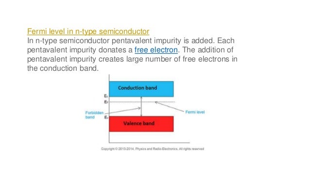
Fermi level in extrinsic semiconductor fermi level in extrinsic semiconductor in extrinsic semiconductor, the number of electrons in the conduction band and the number of holes in the valence band are not equal. The density of electrons in the conduction band equals the density of holes in the valence band. Due to lack of sufficient energy at 0 kelvin, the fermi level can be considered as the sea of fermions (or electrons) above which no electrons exist. The fermi level and fermi energy will be changing depending on the type of material. This is one definition and if we apply concept of fermi level in semiconductors we say it is an energy level between the forbidden band gap (where no electron exists as per the definition) where only the probability is 50%.
Ijlcflwkhxetxm from image.slidesharecdn.com The value for the fermi energy and carrier density is obtained at the crossing (indicated by the arrow) of the two black curves which represent the total positive and total negative charge in the semiconductor. The electrical conductivity of the semiconductor depends upon the total no of electrons moved to the conduction band from the valence band. Likewise, f si e is the fermi level of the semiconductor and si is its work function. Fig.2.7.2 graphical solution of the fermi energy based on the general analysis. Fermi level of extrinsic semiconductor extrinsic semiconductors are formed by adding suitable impurities to the intrinsic semiconductor. Ne will change with doping. The added impurity is very small, of the order of one atom. To a large extent, these parameters are key ingredients that define.
• all energy level in one band is same energy.
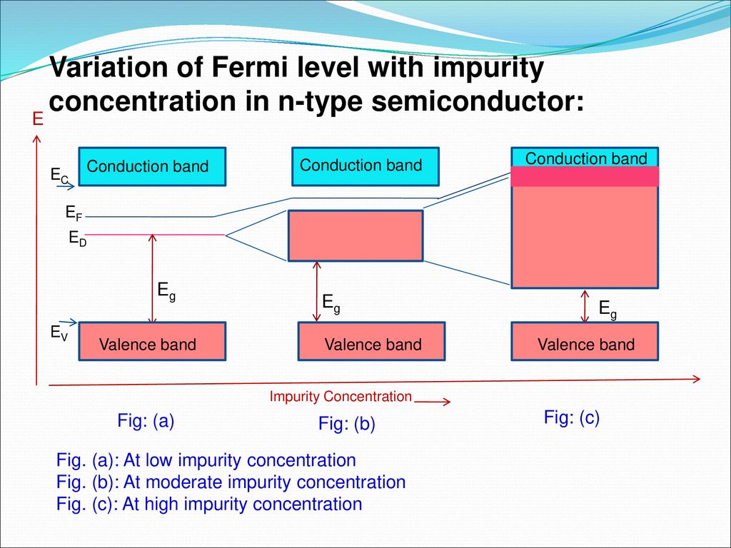
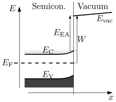
The fermi level is shifted due to doping: The fermi level and fermi energy will be changing depending on the type of material. Fermi level of intrinsic semiconductor. However as the temperature increases free electrons and holes gets generated. Fermi levels, forward bias prof j. Appearance of a contact potential at the interface of a metal and intrinsic semiconductor of course, f m e is the fermi level of the metal and m is the associated work function. Likewise, f si e is the fermi level of the semiconductor and si is its work function. For the intrinsic semiconductor at 0k, The fermi level represents the electron population at energy levels and consequently the conductivity of materials. The electronic properties of semiconductor depend on the number of free electrons and holes available for current conduction. Semiconductor doping and higher temperatures can greatly improve the conductivity of the pure semiconductor material. To a large extent, these parameters are key ingredients that define. (a) fermi level position in pure semiconductors at this point, we should comment further on the position of the fermi level relative to the energy bands of the semiconductor.
In electrical insulators and semiconductors, the valence band is the highest range of electron energies in which electrons are normally present at. Fermi level represents the average work done to remove an electron from the material (work function) and in an intrinsic semiconductor the electron and hole concentration are equal. The fermi level is referred to as the electron chemical potential in other contexts. Why is the fermi level (energy) shfited in doped semiconductors? Kb is the boltzmann constant.
Semiconductor Physics Department Of Applied Physics Ppt Download from slideplayer.com Fermi level lies in the midway between the valence band top and conduction. Fermi levels, forward bias prof j. The density of electrons in the conduction band equals the density of holes in the valence band. The fermi level and fermi energy will be changing depending on the type of material. Fermi energy is the difference highest occupied state and lowest occupied state at 0k. Carrier concentration and fermi level. Smith context the first part of this lecture is a review of electrons and holes in silicon: For the intrinsic semiconductor at 0k,
Fermi level in extrinsic semiconductor fermi level in extrinsic semiconductor in extrinsic semiconductor, the number of electrons in the conduction band and the number of holes in the valence band are not equal.
Semiconductor doping and higher temperatures can greatly improve the conductivity of the pure semiconductor material. Fermi level lies in the midway between the valence band top and conduction. When many li atoms, for example, form a solid, the individual. Kb is the boltzmann constant. However as the temperature increases free electrons and holes gets generated. The fermi level is the surface of fermi sea at absolute zero where no electrons will have enough energy to rise above the surface. Fermi levels, forward bias prof j. The fermi level represents the electron population at energy levels and consequently the conductivity of materials. Ec is the conduction band. If the temperature will be maintained at. The density of electrons in the conduction band equals the density of holes in the valence band. Fermi level in extrinsic semiconductor fermi level in extrinsic semiconductor in extrinsic semiconductor, the number of electrons in the conduction band and the number of holes in the valence band are not equal. To a large extent, these parameters are key ingredients that define.
The fermi level lies between the valence band and conduction band because at absolute zero temperature the electrons are all in the lowest energy state. Ec is the conduction band. Appearance of a contact potential at the interface of a metal and intrinsic semiconductor of course, f m e is the fermi level of the metal and m is the associated work function. I.e., different materials will have different fermi levels and corresponding fermi energy. The concept of fermi level and the fermi energy are the most important topics to be studied in semiconductor physics to attain a detailed understanding regarding band.
Work Function Wikiwand from upload.wikimedia.org Carrier concentration and fermi level. Whenever the system is at the fermi level, the population n is equal to 1/2. To a large extent, these parameters are key ingredients that define. If the temperature will be maintained at. Fermi level of intrinsic semiconductor. In electrical insulators and semiconductors, the valence band is the highest range of electron energies in which electrons are normally present at. As you know, in an atom, certain energy levels are filled, while others are empty. The density of electrons in the conduction band equals the density of holes in the valence band.
The fermi level is at e / u = 1 and k t = u.
The concept of fermi level and the fermi energy are the most important topics to be studied in semiconductor physics to attain a detailed understanding regarding band. Fermi level in extrinsic semiconductor fermi level in extrinsic semiconductor in extrinsic semiconductor, the number of electrons in the conduction band and the number of holes in the valence band are not equal. The density of electrons in the conduction band equals the density of holes in the valence band. The value for the fermi energy and carrier density is obtained at the crossing (indicated by the arrow) of the two black curves which represent the total positive and total negative charge in the semiconductor. Carrier concentration and fermi level. Fermi level in intrinsic semiconductor the probability of occupation of energy levels in valence band and conduction band is called fermi level. Position of fermi level in intrinsic semiconductors • width of conduction band and valence band is small as compared to forbidden energy gap. The electrical conductivity of the semiconductor depends upon the total no of electrons moved to the conduction band from the valence band. Smith context the first part of this lecture is a review of electrons and holes in silicon: The fermi level is at e / u = 1 and k t = u. Fermi level in extrinsic semiconductor 1. The fermi level is shifted due to doping: Fermi level represents the average work done to remove an electron from the material (work function) and in an intrinsic semiconductor the electron and hole concentration are equal.